Product Overview
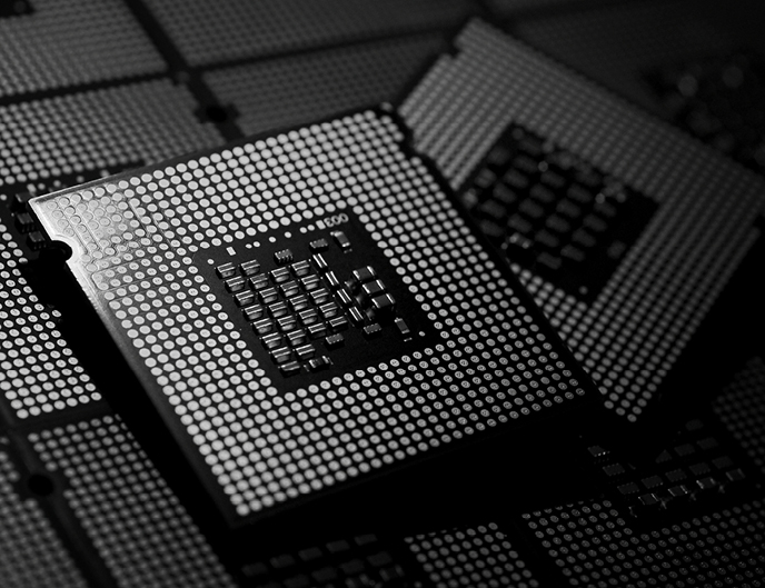
Making through holes and blind vias conductive, while physically strengthening the package, is a challenge faced by IC substrate manufacturers. For electroplating metallization, whether you are building 2 in 1 RDL’s, filling copper through holes or vias, or doing advanced panel-level packaging designs, MacDermid Alpha has an offering to meet every requirement. With a wide array of chemistries designed to work flawlessly together, our innovative solutions for copper electroplating of IC substrate fine lines, vias and through holes delivers unmatched flexibility, capability, and reliability.
Product Features
- 2-in-1 RDL plating with high coplanarity and low trace profiles
- Copper through hole filling for core layer through holes and thermal management
- Embedded trace substrate plating for fine line outer layers
- High speed copper pillar plating
Making through holes and blind vias conductive, while physically strengthening the package, is a challenge faced by IC substrate manufacturers. For electroplating metallization, whether you are building 2 in 1 RDL’s, filling copper through holes or vias, or doing advanced panel-level packaging designs, MacDermid Alpha has an offering to meet every requirement.
Systek Advanced Packaging Brochure (EN)

Systek ETS 1200 Sales Sheet (EN)
Systek UVF 100 Sales Sheet (EN)

Copper Pillar Plating Systems High Speed - Low Heat Technical Publication SMTAI 2017 (EN)
Copper Pillar Plating Systems Technical Publication SMTAI 2018 (EN)
Process Improve Strategies for Weak MicroVia Interface Technical Publication APEX 2021 (EN)
Systek THF Series Sales Sheet (EN)
Systek UVF
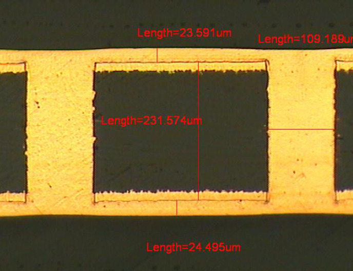
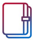
Redistribution layers in IC substrate manufacturing require metallization of fine structures such as blind microvias, X-vias, and fine lines and pads. Systek UVF Series allows 2-in-1 RDL plating of these features in a single bath. The precise chemical system fills blind microvias and X-vias with minimal dimples or overfill, eliminating concerns of dielectric thinning and providing an excellent base for stacking. At the same time, the process also plates lines, pads, and other surface features with high coplanarity and low trace profiles.
Systek ETS Embedded Trace / RDL Substrate Plating
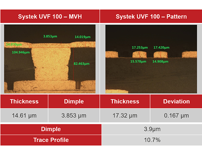
Systek ETS 1200 is an advanced DC acid copper pattern plating process specifically formulated to plate fine lines and pads in embedded trace substrates and redistribution layers. The Systek ETS 1200 process excels at plating the trace profile tolerances and coplanarity requirements of die to IC substrate interfaces allowing R-values below 2 µm for lines and spaces as low as 5/5 µm. The deposit exceeds IPC Class III standards.
Systek MV 400
Systek MV 400 is a DC acid copper pattern plating process specifically designed for 2 in 1 RDL applications. Systek MV 400 consistently fills vias without voids and plates surface features like traces and pads with excellent coplanarity in a single step at high current densities. The production proven 3 component system is fully CVS analyzable.
Systek THF Series
Systek THF Series is a copper through hole filling process that enables improved thermal and structural designs for IC substrates. Systek THF Series provides a solid copper filled through hole in core PCB layers that has higher thermal conductivity than paste without thermal expansion commonly encountered with other materials. The process can fill through holes in a fraction of the time that would be required by direct current plating with minimal dimple and no need for surface planarization, simplifying the addition of subsequent build-up layers.