Product Overview
Our integrated leadframe product portfolio incorporates connected solutions, which span the entire process of building QFN packages from leadframe roughening to enhancing sidewall solderability, and nearly everything in between. Leadframe packages are evolving into a state-of-the-art technology due to their robust reliability and great improvement on performance. With automotive electronics expanding at a rapid rate, leadframe packages like QFNs, QFSs, and DIPs will soon be deployed in new environments that demand the highest reliability. We offer a range of innovative products that enhance reliability of these metal substrate packages.
Product Features
- Decades of industry expertise
- Technology enabling solutions for thinner, faster devices
- Specialty application and technology enabling solutions
Our integrating leadframe packaging portfolio incorporates connected solutions which span the entire process of building QFN packages from leadframe roughening, to enhancing side wall solderability, and nearly everything in between.

Semiconductor Leadframe Packaging Brochure (EN)

HELIOFAB AG 7921 Sales Sheet (EN)
PackageBond Sales Sheet (EN)
PackagePrep Sales Sheet (EN)

A Process for Improved QFN Reliability Technical Publication SMTAI 2014 (EN)
Optimization of die attach to surface-enhanced leadframes for MSL-1 performance of QFN packages (Part 1) Technical Publication Chip Scale Review 2017 (EN)
Optimization of die attach to surface-enhanced leadframes for MSL-1 performance of QFN packages (Part 2) Technical Publication Chip Scale Review 2017 (EN)
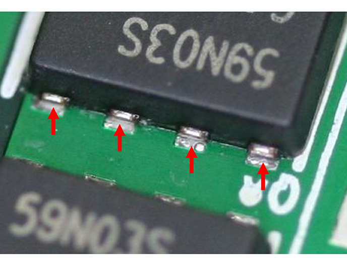
Solderable Finish for QFN Sidewalls
Exposed copper at the singulated edge of QFN packages often solders poorly, preventing conventional solder fillets from forming. The lack of a visible solder fillet inhibits recognition by automated optical inspection (AOI). This reduced solder footprint of the package creates a reliability risk, limiting end-use applications. PackagePrep CE Tin S solves these problems. The highly solderable immersion tin deposited by PackagePrep on the QFN package sidewall allows solder to wick up during paste reflow, creating perfectly formed solder fillets. These fillets can supplement or replace x-ray inspection because they are easily inspectable by AOI. Components that operate in harsh environments must meet more stringent demands than other components. PackagePrep enables a low cost, high reliability solution to the strict requirements placed upon QFN packages in automotive applications.
Proven Reliability at MSL-1 Without Delamination
PackageBond is the no-risk adhesion promotion system specifically engineered for reliability for today’s intense lead-free circuit assembly temperatures. Production-proven in high-volume at premier semiconductor manufacturing facilities, our advanced laboratory innovations deliver extreme heat tolerance to leadframe packages. PackageBond is the advanced leadframe adhesion technology that is designed to overcome delamination problems to achieve MSL-1 reliability. The PackageBond HT-U process improves the bond between the epoxy mold compound and copper leadframe by the micro-roughening of the copper surface and the deposition of an organo-metallic coating to prevent delamination caused by moisture sensitivity or coefficient of thermal expansion (CTE) mismatch.
Adhesion Promotion for Leadframes
PackageBond features patented chemistries that prevent delamination failure of molded packages due to moisture/reflow sensitivity. The process roughens copper alloy leadframes to maximize resin and encapsulant adhesion, plus deposits a thin adhesion booster for long-term delamination protection. PackageBond does not degrade Ag or Ni/Pd/Au plated leadframes, leaving these surfaces clean for predictably strong wire bonds. Production results confirm consistent compatibility with die attach adhesives and no adverse effects on resin bleed.
Plating on Package/Antenna on Package
The PackagePlate processes are a series of plating processes and technologies for metallizing the specially-activated LDS-grade epoxy mold compound that is molded onto semiconductor packages. The plating on package process is based on molded interconnect technology and allows for integration of circuitry inside and on top of the epoxy mold compound. The PackagePlate processes can be utilized to incorporate a number of different functional features within or on the surface of an IC package. The PackagePlate process can be used to form redistribution layers (RDL) from the die to the leads as well as integrate thermal management features internally or externally. It can also incorporate microvias to connect die pads to circuits or antennae (internal or external), and form integrated EMI shielding (internal or external).
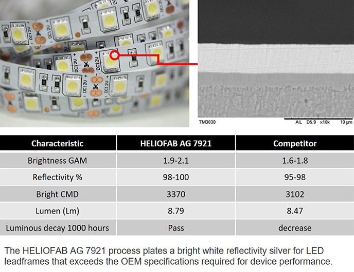
High Brightness Spot Silver Plating for Leadframe LEDs
HELIOFAB® AG 7921 is a spot silver electroplating solution for LED leadframes that delivers a bright white finish with excellent functional properties that can save manufacturers on operational costs versus standard rack plating.
HELIOFAB AG 7921 consistently deposits highly reflective silver with measured GAM values around 2.0 over a wide current density window of 10 to 70 ASD. The deposit does not degrade under luminous decay performance testing, and provides excellent die attach solderability and gold wire bondability.