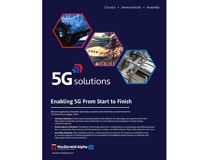
Circuitry Solutions for All Kinds of 5G Devices
High-speed signals, faster processing, and improved performance are delivered by our suite of 5G circuitry solutions. The rollout of 5G adds staggering complexity and challenges to the electronics manufacturing supply chain. Between the ever increasing functionality and device counts on mobile boards, as well as the build-out of new high speed cellular technology and cloud services, solutions for high-density and high-speed circuitry are leveraging more than ever.

Our circuitry solutions products in the 5G supply chain create high-speed, high-density circuitry for devices of all kinds. From mobile devices, cloud computing, network infrastructure, and everything in between, we offer a suite of processes that create value for fabricators. Applications include high-speed innerlayers, molded interconnect devices, primary metallization, electrolytic copper via filling, and solderable final finishes.
High-Speed Innerlayers
Protecting high speed signals from loss can be a challenge. We offer a suite of products to solve these issues in this complex manufacturing environment.
- M-Speed HF – Surface treatment for high-speed copper innerlayers that improves signal integrity at high speeds.
- M-Speed One – Innerlayer dry film adhesion promotion system for high-frequency boards.
Molded Interconnect Devices
Molded catalyst-bearing plastic circuitry for creating 3D circuit structures for a wide array of applications in mobile and chip packing.
- MID Series – Industry-leading portfolio of metallization solutions for LDS-grade molded devices.
- PackagePlate – Suite of plating processes for metallization of LDS grade epoxy mold compound for new 3D packaging integration technology.
Primary Metallization
Our broad portfolio of electroless coppers and direct metallization solutions allow fabricators to initiate plating on nearly any board material with excellent circuit uniformity.
- Shadow® – Graphite-based direct metallization with unmatched compatibility on exotic laminate materials.
- Blackhole® – Carbon-based direct metallization with low etch technology allowing for high yield fine line mSAP.
- M-Copper EF – Electroless copper for horizontal PTH that enables complete coverage in a single pass.
Electrolytic Metallization
For electroplating copper structures onto printed circuit boards (PCBs), from via filling to through hole plating and filling for all board types, we have your solution.
- MacuSpec™ VF-TH Series – Simultaneous via filling and through hole plating for HDI.
- MacuSpec AVF Series – Advanced copper micro via filling solutions.
- MacuSpec PPR Series – Pulse plating electrolytic copper for high aspect ratio multilayer boards.
- Systek THF Series – Copper through hole filling for thermal management.
Final Finishes
Solderable final finishes that have excellent functional characteristics and shelf life.
- Entek® Plus HT – Organic solderability preservative that has excellent reflow performance.
- Sterling® Silver – Immersion silver final finish with low loss for high frequency transmission for PCBs.
- ORMECON® CSN – Immersion tin final finish approved by global OEMs and end users.
IC Substrates
The pinnacle of circuitry is at the interface between these highly dense PCBs and the silicon chips that power today’s devices.
- Systek™ SAP – Semi additive process for circuit formation of the finest IC substrate line and space dimensions.
- Systek UVF – 2 in 1 plating of RDL fills vias and places fine line traces in a single step.
- Systek ETS – Embedded trace substrate plating down to 5/5 micron line and space.
For a complete offering of our 5G solutions, click the link below.