Application Overview
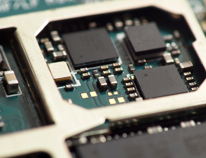
Heterogenous integration using System in Package (SiP) and advanced packaging technology enables the creation of package system solutions with lower costs, higher yields and faster time to market.
A typical SiP may contain passives components, die of different semiconductors such as Si, SiC, GaAs, GaN, Micro-Electro-Mechanical Systems (MEMS), optical components, and other packages such as Quad-Flat No-Leads (QFNs) or Chip Scale Packaging (CSP).
Various process technologies and material solutions are required to integrate the many functions into a SiP.
Interconnect Technology for SiP
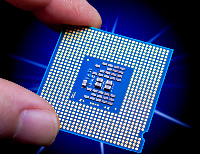
The main purpose of SiP is to combine different functionalities into one package, thereby offering system-level performance in the form factor of a single package. Key processes required for SiP:
- Die attach/stacking
- Wire bonding
- Flip chip attach
- Component/passive attach
- Encapsulation/molding
- Solder sphere attach