Featured Products & Processes
Leadframe Packaging
- Decades of industry expertise
- Technology enabling solutions for thinner, faster devices
- Specialty application and technology enabling solutions
Electrolytic Copper Through Hole Plating
- High throw DC portfolio enables pulse-like plating in DC equipment
- MacuSpec HT series DC baths offer throwing power of greater than 80% at 30 ASF
- Pulse plating portfolio offers superior microdistribution with wide operating windows
- Industry recognized pulse baths including MacuSpec PPR, MPR, and PC 600
Shadow®
- Lowest particle size for fine feature performance
- Unsurpassed reliability verified with IST, OM, Via-Pull, HATS and Thermal Cycling
- Copper via fill plating with no flash plate, improving production flow and cost models
- Simple, easy to control, four step process enables higher throughput
- High copper-to-copper direct bonding strength
BROWSE PRODUCTS & PROCESSES BY CATEGORY

Connectors and Interconnect Finishes
Chemical processes for the application of long lasting corrosion resistant coatings for connectors and interconnects.
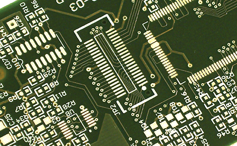
Copper Adhesion Promotion
A wide portfolio of chemical treatments for the copper surfaces that make up the circuitry of printed circuit boards and IC substrates.
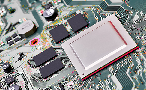
Electrolytic Copper
A full portfolio of acid copper products that meet all applications, from ultra aspect ratio conformal plating down to filling the smallest blind microvias.
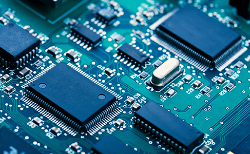
Final Finishes
Our industry leading portfolio of surface preparation and plating processes make us the market choice for organic and metallic final finishes.
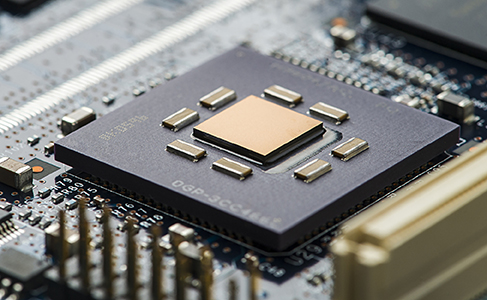
IC Substrates
Our IC substrate solutions today enable the high density designs of the future.
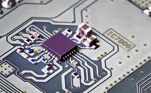
Leadframe Packaging
From specialty applications to technology-enabling solutions allowing for thinner, faster devices, we have everything you need to bridge the performance gap to your next-generation product.
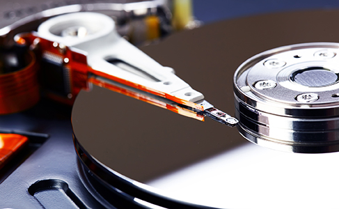
Memory Disk
The world's largest manufacturer of electroless nickel chemistry for memory disk applications.
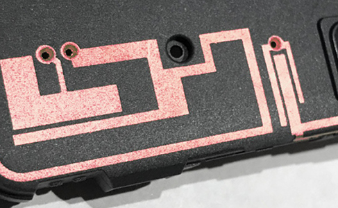
Molded Interconnect Devices
MID plating solutions specifically optimized to deliver precise selectivity, high yields, and ease-of-use for laser direct structured, catalytic ink, and double-shot molded interconnect devices.
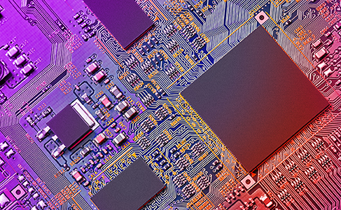
Primary Metallization
Through continued innovation, we develop new solutions to meet the ever-changing electronics manufacturing landscape.
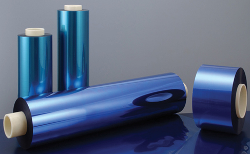
Process Chemistry
We provide innovative chemistries to aid in all aspects of printed circuit formation.
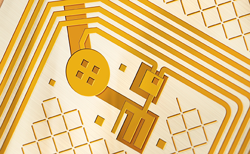
Selective Dielectric Plating
Printing and plating process utilizing proven technology that can satisfy the demand for high volume advanced circuitry.

