The Carbon Footprint of HDI: Direct Metallization vs. Electroless Copper

Over the past year, we have seen printed circuit board manufacturers encounter challenges associated with environmental regulations, water and power outages, and pressures from the supply chain to reduce environmental footprints.
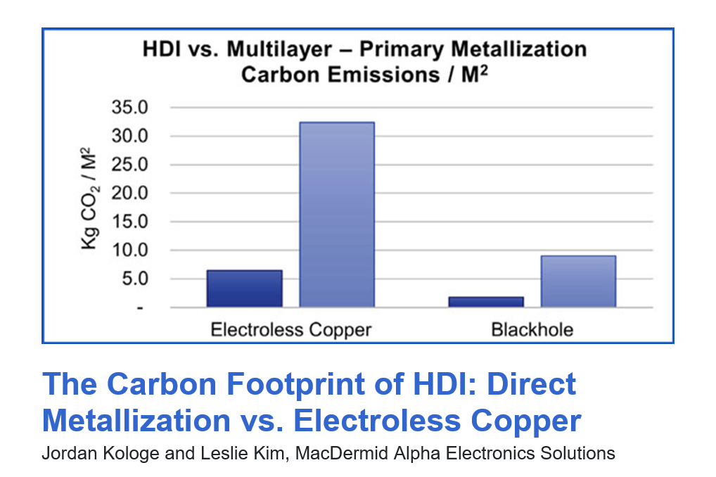
From the perspective of a board fabricator, especially one that specializes in HDI, a highly resource-intensive step in the process of making a printed circuit board is the primary metallization step. All circuit boards that have multiple layers go through such a primary metallization, which is either electroless copper or direct metallization (DM). The main difference between a direct metallization process and the more traditional electroless copper plating process is that the former deposits a paint-like conductive coating through absorption onto the surface, while the latter deposits a copper coating from solution through chemical reduction. The DM coatings are most typically a carbon or graphite, and this kind of board manufacturing has been done reliably for nearly four decades. Click here to read the full article.