Safer and Healthier Die Bonding with PFAS-Free Die Attach Adhesives

Authored By

 Download This Article
Safer and Healthier Die Bonding with PFAS-Free Die Attach Adhesives
In this insightful paper, Senthil Kanagavel delves into the pivotal shift toward PFAS-free die attach adhesives in the fabrication of wire bond semiconductor packaging. He begins by detailing the history of PFAS, highlighting environmental and health concerns and the increasing regulatory restrictions driving the urgency of this transition. Senthil then explores the evolution of the semiconductor packaging industry and the role PFAS has played in die bonding. He then examines challenges faced by packaging houses as they transition to PFAS-free die attach materials and concludes by offering a roadmap for success, guiding industry professionals through this critical change.
Greener Electronics
In my work, I support the development of sustainable material solutions for the electronics industry. Historically, materials were developed for reliability and mechanical, electrical and thermal performance – crucial factors in electronics. Today, however, we have an added mission: to help the electronic industry reduce its environmental impact.
Research and development efforts must now blend biology, ecology and recyclability with traditional disciplines like chemistry, physics and thermodynamics. Plus, we must keep up with ever-evolving environmental, health and safety regulations. With this in mind, let’s dive into the fascinating topic of “forever chemicals” known as PFAS.
PFAS Unveiled
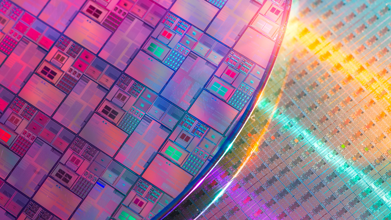
PFAS (Per- and Polyfluoroalkyl Substances) are a large group of synthetic chemical compounds characterized by strong fluorine-carbon bonds, which provide exceptional durability and toughness. These properties make PFAS useful in numerous industrial and consumer applications. Since their discovery in 1938, thousands of PFAS compounds have been developed, including long-chain PFAS polymers and short-chain low-viscosity PFAS mixtures. These compounds have been incorporated into a wide range of products, including cosmetics, food packaging, non-stick cookware, fire- and moisture-resistant materials, seals, hoses, wires, cables and electronics.
PFAS are referred to as “forever chemicals” because they are virtually indestructible and don’t break down in the environment. This durability has led to their persistence in soil, water and air, as well as their bioaccumulation in plants, wildlife and the human body over time. This persistence is concerning due to potential adverse health effects. Research has linked exposure to certain PFAS compounds to various health issues.

The Rise of PFAS Pollution Awareness and Regulations
PFAS were not widely documented in environmental test samples until the early 2000s. Since then, detecting PFAS in the environment has become major focus of research. Advancements in analytical testing methods have increased test sensitivity, leading to a rise in reported PFAS detections in soil and drinking water supplies worldwide.
Growing environmental and health concerns have led to a significant push to reduce PFAS manufacturing and usage globally. Litigation and country-specific regulations are on the rise, driving the transition to sustainable alternatives. The most recent developments have been:
- February 2023: The European Chemicals Agency (ECHA) proposed a ban on production and import of PFAS compounds under EU REACH Annex XVII restricted substance list. The EU is expected to adopt the proposal in 2025.
- April 2024: The U.S. EPA accelerated the pace of research and actions to legally enforce drinking water standards and protect communities from exposure to harmful PFAS compounds. Concurrently, the EPA announced $1 billion in funding to help states implement PFAS testing and treatment at public water systems to address PFAS contamination.
- July 2024: Canada prohibits the manufacture, use, sale, offer for sale and import of three subgroups of PFAS.
These highlight the increasing wake-up call and response to the hazards of PFAS pollution worldwide.
The Tale of PFAS in Wire Bond Semiconductor Packaging
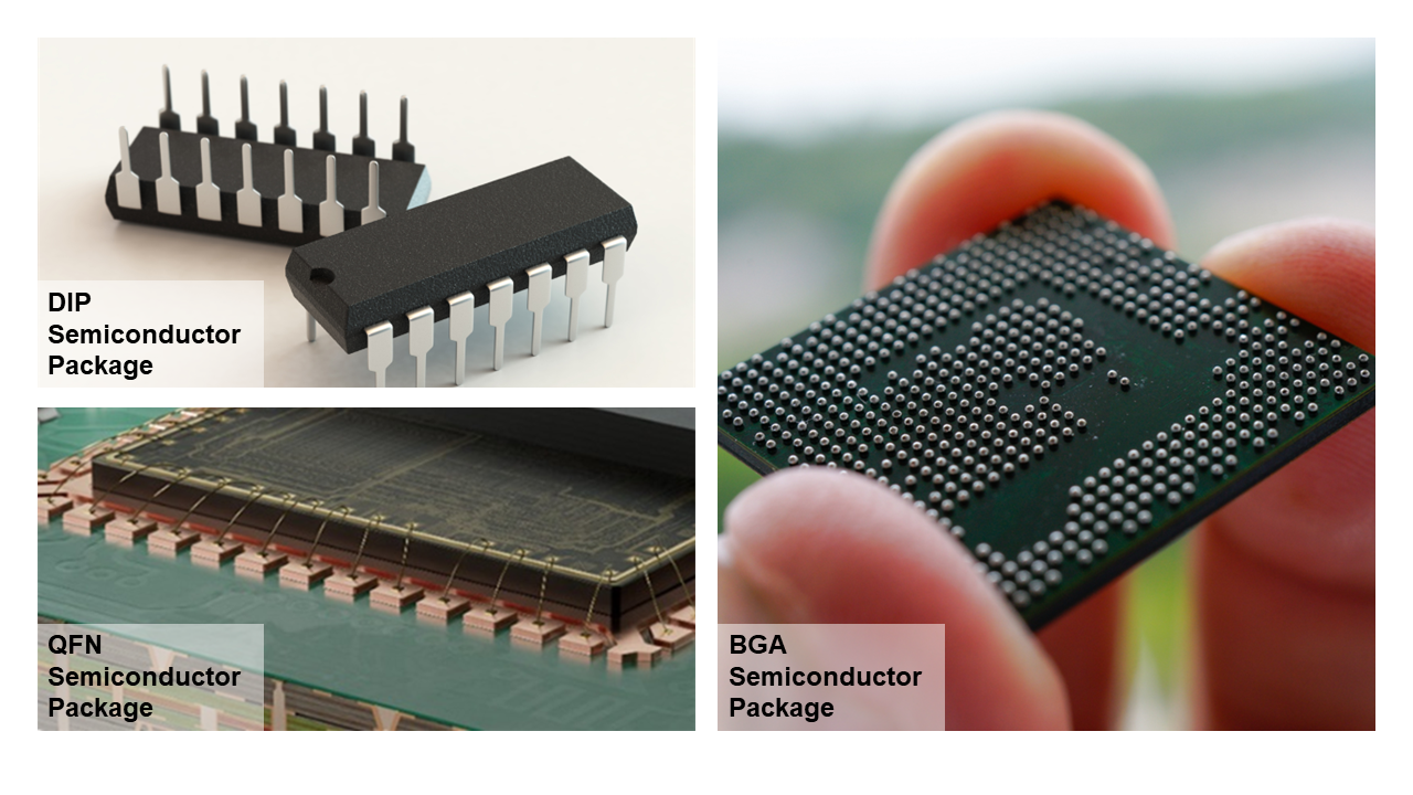
Since the introduction of the Dual In-Line Package (DIP) in the 1970s, semiconductor packaging technology has evolved to meet the demand for higher pin counts and smaller footprints. For example, the Ball-Grid Array (BGA) from the 1990s and the Quad Flat No Leads (QFN) from the 2000s both use wire bond interconnect technology, which continues to be widely used today. Wire bond semiconductors require a specific type of package to encase the integrated circuit (IC) or chip, its carrier and delicate connecting wires1.
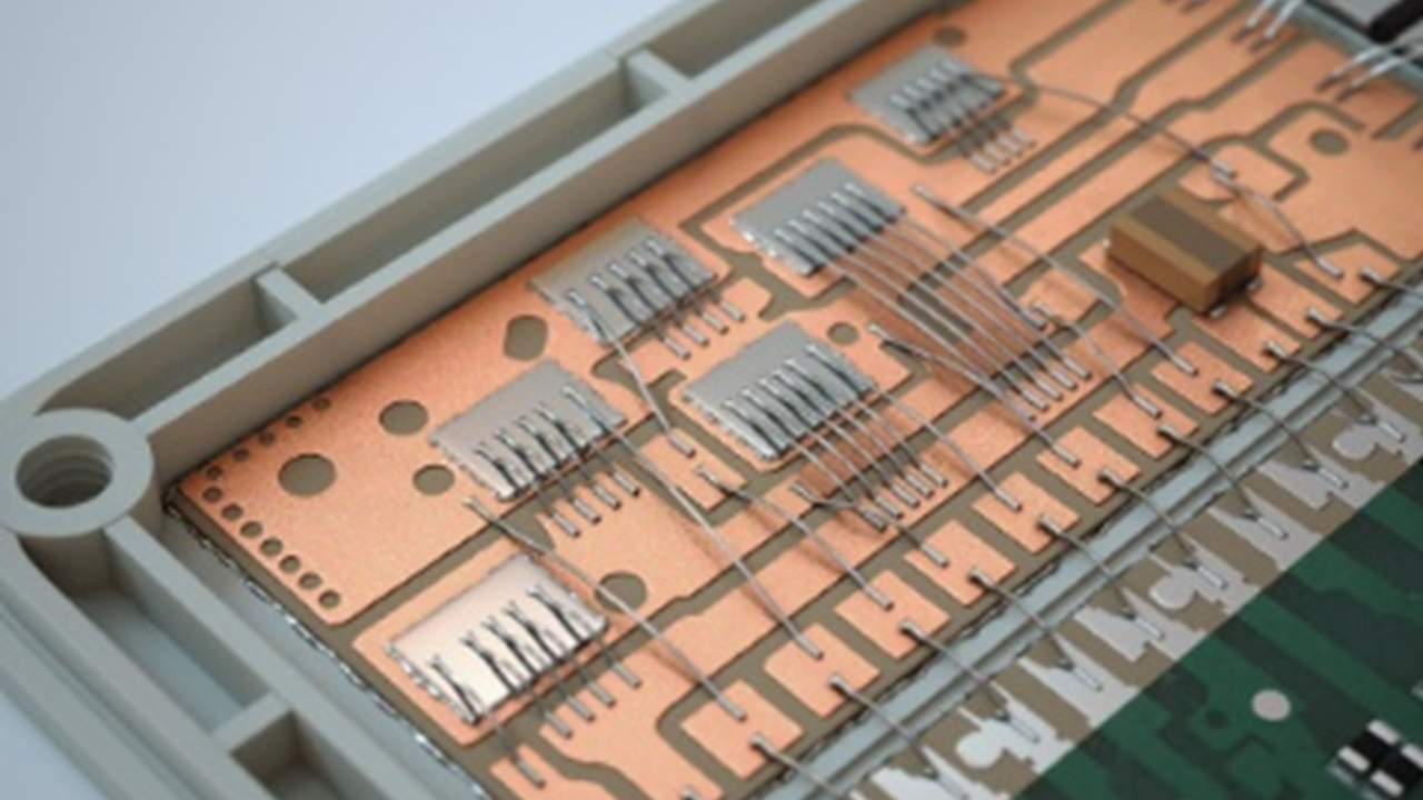
A critical step in the wire bond packaging process is bonding the chip to the die pad or substrate. Die attach adhesives are formulated to serve multiple essential functions:
- Strong Adhesion: Die attach adhesives secure the silicon chip to the metallized die pad.
- Electrical Connectivity: Conductive die attach adhesives facilitate electrical conductivity, serving as a ground plane for the package.
- Thermal Management: Conductive die attach adhesives enhance the transfer of heat away from the chip, preventing overheating and improving longevity.
- Mechanical Support: Die attach adhesives provides structural support, protecting the chip and its connections from shock and vibration during handling, assembly and operation.
Since the 1970s, long-chain PFAS polymers have been added to die attach adhesives to enhance bond strength and durability, as well as improve environmental, mechanical and thermal performance.
PFAS-based die attach adhesives are still in use today. However, with increasing regulatory pressures to reduce or eliminate PFAS, the next logical evolutionary step in wire bond semiconductor technology is the transition to PFAS-free die attach materials.
The Path to Change: Challenges and Hurdles
Transitioning from PFAS-based die attach adhesives, which have been used for decades, to environmentally sustainable alternatives can be a daunting task.
The first challenge semiconductor packaging houses typically face is identifying which die attach materials in their supply chain contain PFAS. Conducting a thorough audit for PFAS content is crucial. This can be achieved by obtaining certificates of compliance, test reports, material disclosures and safety data sheets from material suppliers, paying close attention to any mention of PFAS or fluorine content. In some cases, collaborating with a testing laboratory to perform material analysis may be necessary.
The next hurdles involve identifying and validating PFAS-free alternatives for specific applications. Finding suitable alternatives can be time-consuming and resource-intensive, especially in industry sectors with strict qualification requirements. Once alternatives are identified, they must undergo rigorous testing to ensure they meet the necessary performance standards.
The move to PFAS-free die attach adhesives is inevitable due to regulatory restrictions in Europe, U.S. and Canada (outlined above). Many companies are in the process of proactively investing in the transition, working with their suppliers to overcome challenges, and lead the industry to a more sustainable future.
Team Up with Pros!
Navigating regulatory and supply chain complexities requires making difficult choices. Introducing new materials into an existing large-volume manufacturing process is challenging and demands careful consideration.
Partnering with an expert supplier, like MacDermid Alpha, can ease the transition. As a global leader in the electronics materials industry, MacDermid Alpha is dedicated to environmental responsibility and recognizes the importance of proactively addressing regulatory concerns.
In 2008, our team began developing PFAS-free adhesives for die bonding. Today, MacDermid Alpha Electronic Solutions offers a comprehensive portfolio of PFAS-free solutions.
Our portfolio of PFAS-free die attach solutions include:
- ATROX® Conductive Die Attach Paste: Offering excellent bond-ability to a variety of lead frame surfaces and die sizes.
- ATROX® Hybrid Silver Sintering Die Attach Adhesive: Ideal for high power semiconductors and exposed pad semiconductor packages.
- ALPHA® ARGOMAX® Sinter Silver Paste: Printable paste developed for pressure sintering of large packages on gold and silver finish substrates.
- ALPHA® ARGOMAX® Sinter Silver Film: Designed for die-transfer-film processes on gold and silver surfaces using existing pick and place equipment.
These groundbreaking materials are safer, higher-performing alternatives compared to traditional PFAS-based die attach adhesive materials, and they are readily available to meet your high-volume manufacturing needs.
Want to learn more? Request a consultation - we are here to help!