
What is a Photomask?
A photomask is a quartz or glass substrate, coated with an opaque film in to which is etched the design of the device being manufactured.
The photomask plays a critical role in the microlithography process used by our customers for the manufacture of integrated circuits (ICs), photonic devices, and micro-electro-mechanical systems (MEMS). A photomask consists of a fused silica (QZ) or, glass (SL) substrate coated with an opaque film, in to which an accurate replication of the device designer’s pattern is etched. In addition to a high degree of pattern fidelity, the photomask also has to meet our customers’ expectations for linewidth (critical dimension or CD) control, pattern placement (registration), and defectivity control. The terms ‘masters’, ‘sub-masters’ and ‘copy masks’ are usually used to refer to 1x photomask, while the term ‘reticles’ refer to 2.5x, 4x and 5x stepper or scanner photomasks. A functioning device can require between 5 to 40 individual photomasks, one mask for each step used in the fabrication process.
How is a Photomask Used?
While photomasks have a variety of applications, the majority are used to support the microlithography process our customers use.
The photomask image consists of a binary pattern accurately replicating the original design. While photomasks have a variety of applications, the majority are used to support the customers and microlithography process as an intermediate step between design and manufacture of IC, photonics, and MEMS devices.
This binary pattern modulates the intensity of light in the lithography tool being used to ‘print’ the design on to the silicon wafer or other substrate being used.
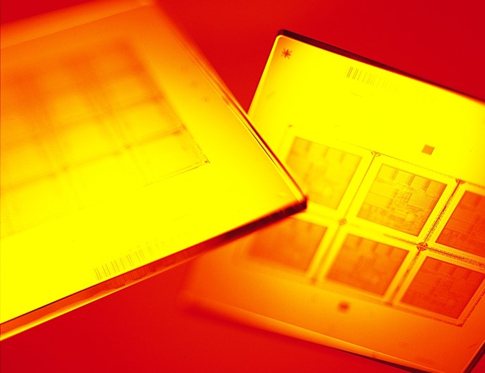
How is a Photomask Made?
They are made by exposing or writing the device designer’s pattern on to a resist coated chrome blank photomask. A photomask is made by exposing, or writing, the designer’s pattern onto a resist coated chrome mask blank. The latent image in the resist is then developed to form the required pattern. This resist image acts as a mask during the etching process. The pattern is transferred into the chrome film when the resist layer is removed. CD’s and pattern placement are measured to ensure they meet our customer’s specifications. The pattern is then inspected for any defects that may affect device functionality, which are repaired if necessary. A final clean, and if required, a protective pellicle is attached to complete the photomask manufacturing process.
Photomask Types
Our customer’s processes and the lithography tools vary significantly. The scale factor (1x through 5x reduction ratios), mask to substrate printing proximity (full contact to close proximity aligners, projection steppers or scanners), and the wavelength of light used (‘broadband’ through to deep-UV), all influence the physical characteristics of the photomasks. Copy Masks When our customers use hard contact printing to transfer the design to their substrates, the photomask can quickly deteriorate due to mechanical damage. When the feature size and specifications allow, the most cost effective solution can be to use a copy photomask made from a ‘master’ or ‘sub-master’ which we retain for making additional copies as required. Copy masks are usually made on soda-lime (SL) glass substrates. 1x Masks When our customers use close proximity printing or projection aligners to transfer the design to their substrates, little or no attrition of the photomask occurs. Like hard contact printing, these systems typically use broadband or near-UV light (300-450nm) to expose the wafer or substrates. While still at the same scale factor (1x) as the final device, higher pattern fidelity and tighter specifications can be met using photomasks made directly by our mask-writers. 1x masks can be made on either soda-lime (SL) glass or fused silica (QZ) substrates. Reticles When our customers use an optical projection stepper or scanner with a reduction ratio of 2.5:1, 4:1 or 5:1, the photomasks used in these systems are usually called ‘reticles’. These systems use single wavelengths from i-line (365nm) to deep-UV (248nm or 193nm). Reduction stepper or scanner reticles, typically support the most stringent lithography requirements. In some of the advanced fabs, they are imaging features smaller than the wavelength of light. Reticles are typically made on fused silica (QZ) substrates.